2024 is going to be a big year for Intel as Intel is trying its best to take back its throne from TSMC foundry business and in that Pursuit Intel unveiled its Backside Power Delivery technology .
We recently covered a detailed article on can Intel’s new 18A process which includes backside power delivery compete with TSMC ,if you have not read that already ,I would recommend you to have a look on that ,here Is the link.
So , the very first question that comes to mind is what the hell is this Backside power delivery?
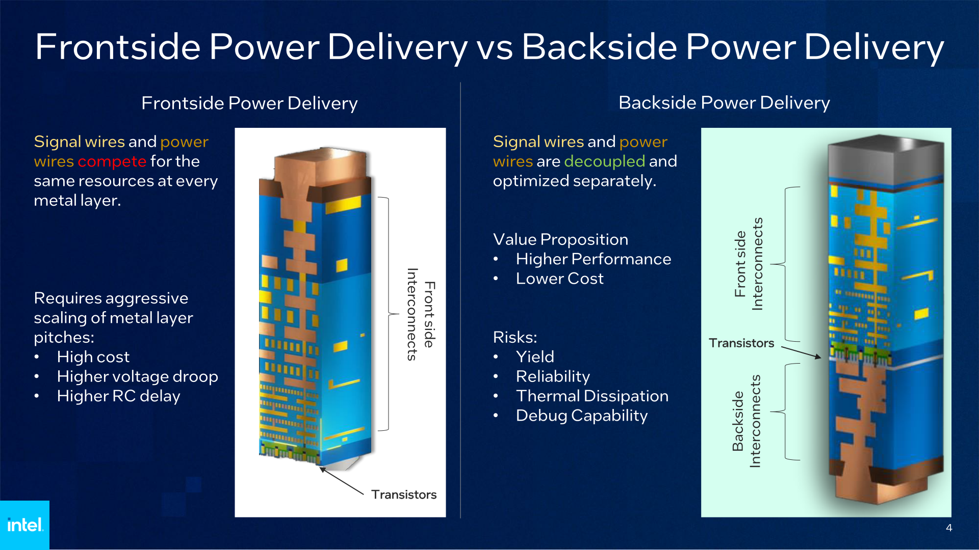
Backside power delivery involves supplying power to the underside of integrated circuits rather than the traditional connections along the edges of the chip. Previously we used to have unified circuitry path for power delivery and signal communication . Due to this the overall area used to increase as well as lead to complications.
This approach provides benefits like improved power efficiency, lower voltage operation, and advanced chip architectures.
Backside power delivery allows for bigger interconnects which results in improved frequencies, reduced switching capacitances and much more transistors in smaller area.
Intel is achieving this with What they call as PoweVia Technology.
So before moving ahead, let us have a look on Intel’s PowerVia Technology
Intel’s PowerVia Technology
Intel has developed a proprietary approach called PowerVia that makes direct connections from the backside bumps down to the transistor contacts. This creates very low resistance paths for power, thus reducing losses.
Reducing losses not only means reduced power dissipation but also means improved thermals, and higher frequency operations. It also avoids using the lower on-chip wiring layers for power delivery.
Benefits of PowerVia
- Frees up space on the front side wires, allowing them to be made thicker. This reduces resistance, capacitance, and inductance, enabling performance gains.
- Avoids aggressive scaling of the lower metal layers, saving costs and complexity.
- Enables easy integration with next-gen transistor technology like RibbonFET.
In the market there are also other technologies who claim backside power delivery, so a question automatically arises …

How PowerVia Stands Apart?….
Intel’s PowerVia takes a different approach to backside power delivery compared to some other companies. Key differences include:
- Direct transistor contact: PowerVia makes direct connections between the backside and transistor contacts. This creates the lowest resistance paths, beyond what secondary metal layers provide.
- No displacement of lower metals: PowerVia doesn’t route through lower metal layers. This avoids consuming routing resources needed for signals.
- Lower complexity: PowerVia has the benefit of simplicity by leveraging Intel’s advanced manufacturing on a single die. Some alternatives rely on separately manufactured dies requiring complex alignment.
- Optimized integration: PowerVia is tailored for integrating with future advances like Intel’s RibbonFET transistors. The synergistic combination drives maximum gains.
- These advantages translate to PowerVia providing better power efficiency, higher performance, lower manufacturing complexity and costs than competing backside approaches.
Whenever a company works on new node or somewhat new technologies ,they have to make tons pf tests to confirms their working and also check whether they are in accordance with their expectations or not ,so lets have a look on validations and results of this PowerVia Technology
Validation and Results
Intel validated PowerVia technology on a 10nm test chip before integrating it on the Intel 20A and 18A nodes. The test chip demonstrated good yield, thermal management, and ability to debug chips with backside power delivery. Performance results show benefits like:
- 90% Cell Utilization
- 30% reduction in power supply losses
- 6% increase in frequency
- 10% area improvement
So now a question arises what are the possible areas where this backside power delivery can actually be useful.
Backside power delivery will come out as a boon for power intensive applications which include Artificial intelligence ,High Performance Computing(H.P.C) , Graphics intensive tasks and obviously Gaming.
The Road Ahead
PowerVia and RibbonFET show Moore’s Law continues, providing major gains for Intel’s 2025 process leadership target. Many options like new channel materials and 3D stacking will further enhance progress after the 20A and 18A nodes.
Conclusion
Backside power delivery and Intel’s PowerVia integration is an important advancement, providing tangible perf/watt/area improvements. Along with ecosystem support, it will enable new generations of products across computing segments.
Discover more from WireUnwired Research
Subscribe to get the latest posts sent to your email.


