Intel recently unveiled details of their newest manufacturing process technology featuring 18A transistors with backside power delivery. This innovation prompts the question – does this finally spell a comeback for Intel’s foundry business in the face of TSMC’s formidable market lead?
What is Backside Power Delivery and Why It Matters?
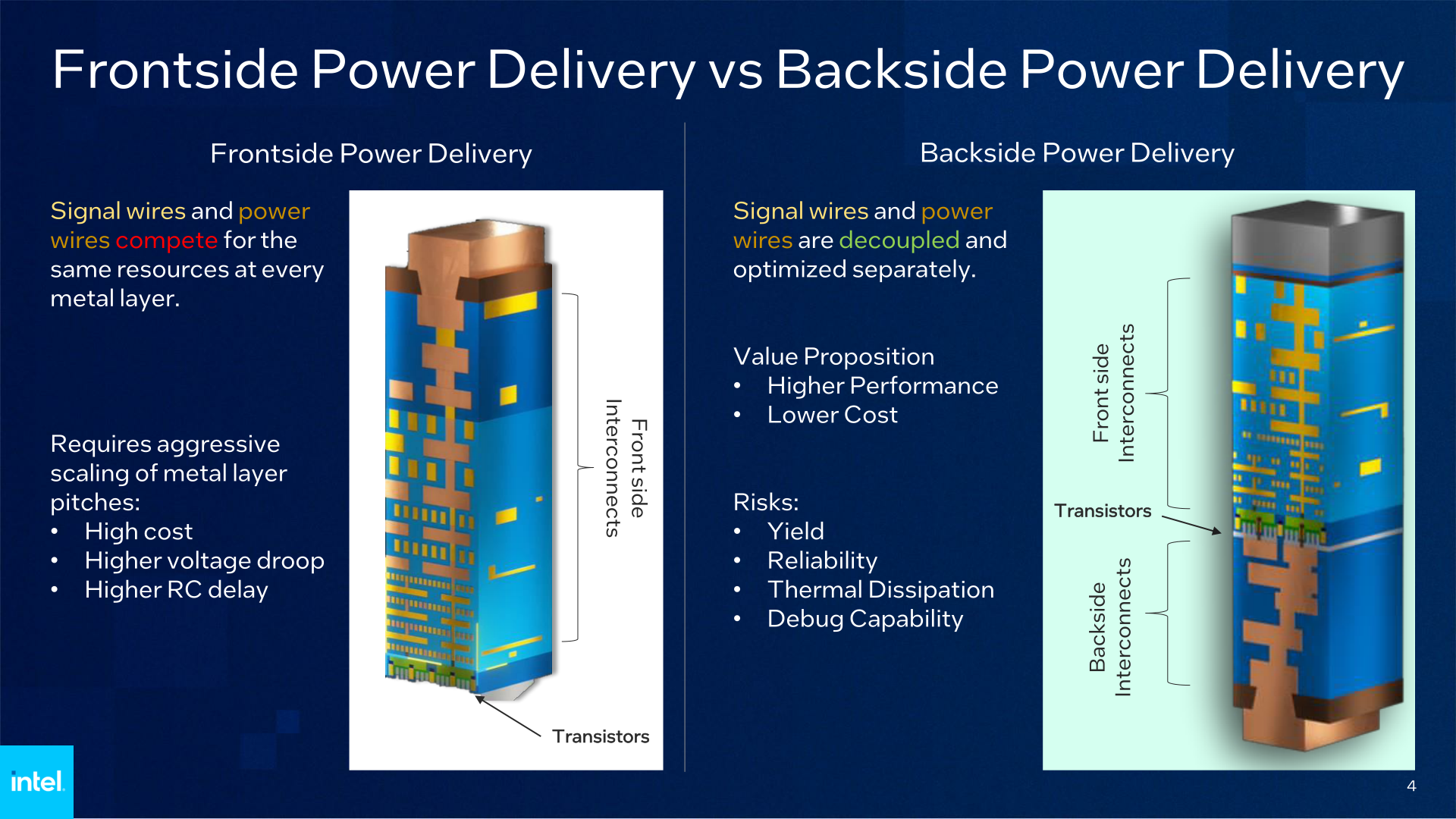
Backside power delivery refers to supplying power to the backside of a semiconductor chip instead of the front side. This innovative approach provides two key advantages:
- Improved Thermal Management: Enables more efficient dissipation of heat generated by chip components
- Higher Overall Performance: Allows optimized delivery of power to chip components, increasing speed and efficiency
Intel’s 18A Process Features Backside Power Delivery
Intel’s new 18 nanometer (18A) manufacturing process introduces backside power delivery to the chip fabrication workflow. The “A” refers to the generation of the process node. This implementation of backside power delivery will be an industry first.
We have covered a whole article on backside power delivery ,if you are interested have a visit

Source :intel
Historically, Intel has spearheaded several pivotal innovations in chip fabrication, like high-k metal gates and 3D FinFET transistors. So while TSMC currently leads the foundry market, Intel’s technical expertise and proven ability to engineer cutting-edge advances positions them as a formidable competitor.
Loving our content and wish to remain updated to daily dose of semiconductor news ?:-Join our Whatsapp Channel
However, truly compelling semiconductor manufacturing requires both innovative technology as well as enduring customer partnerships to translate that technology into products. This poses a potential challenge for Intel.
TSMC Maintains Edge Through Customer Ecosystem and Collaboration Workflow
While Intel focuses on developing advanced but internal chiplet technologies, TSMC concentrates on an open chip fabrication ecosystem that attracts industry-leading customers like Apple, Qualcomm, AMD and others. The result is a reliable, high-volume manufacturing workflow capable of producing customer-designed complex chips at scale.
TSMC also has pioneered advanced packaging techniques thanks to the ability to co-optimize methodologies directly with partners. Intel however currently outsources packaging to TSMC itself.
Excited for India’s semiconductor journey in 2024?
Bridging the Foundry Divide Through Broad Customer Adoption
For Intel to fully revive its foundry business, engineering feats alone may not suffice. The company will need to attract external fabless customers to its backside power delivery-enhanced 18A process in order to demonstrate viability and build market confidence.
If sufficiently compelling, the promise of efficiency and performance gains could entice customers to adopt Intel’s offerings for producing advanced chip designs. This in turn can fuel a self-reinforcing cycle of additional innovation on Intel’s manufacturing side in collaboration with partners.
In that scenario, Intel would have an opportunity to disrupt the foundry landscape and mount a challenge to TSMC’s supremacy in the coming years.
Discover more from WireUnwired Research
Subscribe to get the latest posts sent to your email.


