You must have seen some brightly coloured lines and diagrams in VLSI chip design; have you ever wondered what they are?..
Actually, these colourful lines are what we call a stick diagram and depict the chip’s transistor and interconnection layout.
You can think of it as a blueprint for the physical implementation of the chip. It basically visualises our design and enables the designers to visualise how the components will be laid out and connected on the silicon.
In this very detailed discussion, you will get to know more about these stick diagrams, their uses, and how to draw them from scratch from Boolean functions.
So, without any ado, let’s start learning about these stick diagrams…
TRENDING
What are stick diagrams?
A stick diagram is a schematic diagram of a digital circuit’s transistor layout and connections. It is a design tool that uses lines and rectangles to represent transistors and their connections.
Stick diagrams represent devices and conductors as “sticks” or lines to design the circuit’s architecture, define the direction and metalization of the power supply, ground, input, and output. Stick diagrams are a common approach to symbolic design.
Why Do We Need Stick Diagrams in VLSI?
- Stick diagrams are an easy way to capture topography and layer information. Stick diagrams represent layer information using color codes (also known as monochrome encoding).
- It displays all components/vias (through a metal link that connects higher-level metals).
- It depicts the relative position of components.
- It moves us one step closer to the layout.
- Helps plan the layout and route.
How do we draw CMOS stick diagrams from scratch for Boolean functions?
Let’s understand with the help of some examples.
Suppose we want to draw a stick diagram of a NAND gate.
The NAND gate Boolean expression is F = (A.B)’
Join Our WhatsApp Community.
The complement of F is F’ = ((A.B)’)’, Now we will simplify the expression using De Morgan’s theorem. So F’ = (A.B),
So, according to the rule,
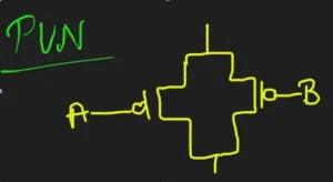
In PMOS, for a dot operation between two variables, A and B, we connect their PMOS transistors in parallel. They will operate as a pull-up network (PUN). As shown in Figure
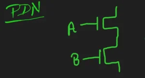
Similarly, in NMOS, we will connect the NMOS transistors of two variables in series to perform a dot operation. They will operate as a pull-down network (PDN). As shown in Figure
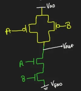
Then, using CMOS logic, we will connect the PUN to the PDN, providing Vdd to the PUN and Vgnd to the PDN. We will also add the Vout, so they will look like the figure below.
Now, we can draw the stick diagram for the above figure by following these steps.
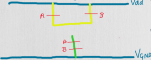
Step 1. We will draw the Vdd and Vgnd rails parallel to each other with blue color.
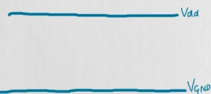
Step 2: We’ll draw the transistors. For PMOS, use yellow to make them parallel and red to cut them horizontally; they will represent the input logic. In this case, red represents Poly.
Similarly, draw a vertical green line for NMOS because our NMOS transistors are in series. Use red to cut them horizontally to represent NMOS transistors.
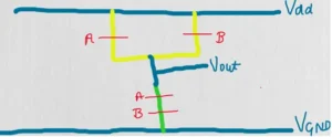
Step 3: We will now use blue to connect PUN and PDN and attach Vout to it.
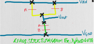
Step 4: We are almost finished, but hold on—most crucially, we will represent each connection with a cross in black.
If you still did not get much , you can see this detailed video on stick diagrams.
Discover more from WireUnwired Research
Subscribe to get the latest posts sent to your email.


