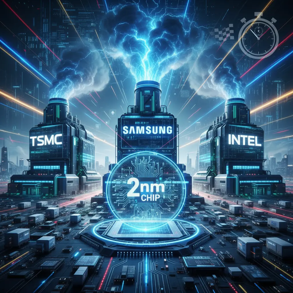
In 2025, the semiconductor industry stands on the brink of a major advancement with the introduction of 2-nanometer (2nm) technology. TSMC began risk production of its 2nm process in mid-2024 and is moving steadily toward mass production in the second half of 2025. Their enhanced N2P process, expected to roll out fully in 2026, features gate-all-around (GAA) nanosheet transistors replacing traditional FinFETs. These innovations enable denser transistor packing, better electron control, reduced leakage, and lower heat output. As a result, compared to current 3nm chips, the 2nm node brings 15-20% higher performance and up to 30% reduced power consumption, allowing devices to be faster and more efficient.
Also Read : TSMC affirms 2nm Chips Production in the U.S By 2028
MediaTek Joins the 2nm Pioneer Club

As TSMC’s 2nm production timeline solidifies through 2025, the first major customer success stories are emerging. Just this month, in September 2025, MediaTek announced it has successfully completed the tape-out of its flagship chip using TSMC’s 2nm N2P process—marking a significant milestone in the practical implementation of this advanced node. This achievement positions MediaTek among the first wave of companies to successfully design and prepare chips for TSMC’s upcoming mass production phase.
The chip, widely expected to be the Dimensity 9600, represents MediaTek’s strategic bet on staying competitive with industry leaders. Volume production is scheduled for late 2026, aligning perfectly with TSMC’s N2P process rollout timeline mentioned in your introduction. This timing ensures MediaTek will have access to the enhanced 2nm process featuring gate-all-around transistors when it reaches full commercial availability.
MediaTek’s successful tape-out demonstrates that the 2nm transition from laboratory to commercial reality is accelerating faster than many anticipated. As MediaTek President Joe Chen noted, their collaboration with TSMC enables flagship chips that “deliver high efficiency across products ranging from edge applications to cloud services”—exactly the kind of versatility that 2nm’s 15-20% performance gains and 30% power reduction make possible.
The Current State of Foundry Competition in Late 2025
While MediaTek celebrates its 2nm milestone with TSMC, the broader foundry landscape reveals an increasingly competitive race as we move through the second half of 2025. TSMC’s early lead becomes apparent in the yield metrics that determine commercial viability: TSMC is achieving approximately 65% yields on their 2nm process, significantly ahead of competitors who are still struggling with lower production efficiency.

Where is Samsung in the 2nm Race ?
Samsung faces mounting pressure as 2025 progresses toward its close. Despite targeting 2nm mass production in this same timeframe, Samsung’s foundry division confronts a series of escalating challenges that have unfolded throughout the year. Early in 2025, Samsung’s SF2 process yields started at just 30%—far below commercial viability. By mid-2025, the company had managed to improve these yields to over 40%, representing meaningful progress but still falling well short of the 60-70% threshold needed for major customer orders.
This yield struggle has created a cascading series of strategic adjustments throughout 2025. Industry sources reveal that Samsung is now racing against a tightening timeline to achieve 70% yield rates within the next six months—a target that would position them for customer wins in early 2026. However, the challenges extend beyond yield rates alone. Testing conducted with major customers like NVIDIA during 2025 has revealed that Samsung’s 2nm chips, while functional, are delivering overall performance including power efficiency that falls short compared to TSMC’s competing offerings.
How is Samsung handling its 2nm crisis ?
To address these competitive disadvantages as 2025 draws to a close, Samsung has implemented an aggressive pricing strategy, offering 2nm services at approximately 30% lower costs than TSMC. This approach has yielded some success—most notably securing a potential $16.5 billion chip manufacturing agreement with Tesla for AI6 chips—but the overall volume remains limited compared to TSMC’s major customer wins.
The cumulative effect of these challenges through 2025 has forced Samsung into a critical strategic pivot. The company announced in September 2025 that it would delay its 1.4nm node from 2027 to 2029, redirecting engineering resources to improve 2nm yields and develop enhanced versions. Moving into 2026, Samsung’s roadmap now focuses on refining its second-generation 2nm process (SF2P) and launching a third-generation version (SF2P+), promising over 20% performance improvement. This timeline compression makes the window of opportunity in 2026 particularly crucial for establishing credibility with major external customers.
How is Intel Doing in this 2 nm race ?
Intel presents the most intriguing wild card as the industry transitions into 2026. Throughout 2024, Intel accelerated its 18A process timeline, moving production up from the original 2025 target to late 2024—a timeline that has proven successful as Intel now claims process parity with TSMC’s offerings. More impressively, Intel’s yields have shown rapid improvement, climbing from 50% to 55% over just one quarter in 2025. If this improvement trajectory continues into 2026, Intel’s 18A process could potentially reach 65-70% yields by mass production—positioning Intel ahead of Samsung foundry while remaining competitive with TSMC’s projected 75% yields.
The practical validation of 18A is already underway as 2025 concludes. Intel’s Panther Lake processors, powered by 18A technology, launched in late 2025, serving as a crucial proof point for the technology’s commercial viability. Building on this foundation, Intel has developed 18A-P, a customer-facing variant that will enter mass production in H2 2026 specifically for foundry customers. This timing could prove pivotal, as 18A-P appears competitive with TSMC’s N2 process while offering an alternative supply source for customers concerned about TSMC capacity constraints.
Intel is moving for its 14A process ?
Looking beyond 2026, Intel’s roadmap reveals even more ambitious plans. The company’s 14A process, targeting 2027-2028, represents a potential technological leapfrog with revolutionary capabilities. 14A will be Intel’s first node to utilize ASML’s $380 million High-NA EUV lithography machines—a significant upgrade from the $235 million tools used in current processes. Combined with advanced RibbonFET 2 transistors, PowerDirect backside power delivery, and innovative “Turbo Cells” technology, 14A promises 15-20% better performance-per-watt and 25-35% lower power consumption compared to 18A.
However, Intel’s ambitious timeline faces a critical dependency that will be resolved in 2026. The company has explicitly stated that 14A development will only continue if they secure significant external foundry customers—creating a high-stakes gamble tied directly to 18A-P’s market success. Early indicators suggest promise, with several companies evaluating 14A and the US government committing to Intel for defense and space chips. Yet the semiconductor industry will closely watch throughout 2026 whether Intel can convert these evaluations into the volume commitments needed to fund 14A’s completion.
The stakes for Intel’s foundry ambitions could not be higher as the industry enters 2026. Success with 18A-P could establish Intel as a credible TSMC alternative, while 14A’s advanced technologies might enable technological leadership by 2027-2028. Failure, however, could force Intel to pause advanced node development and rely on external foundries like TSMC for future processors—a strategic reversal that would fundamentally reshape the competitive landscape through the end of the decade.
Where are Fabless Giants in this 2 nm race ?
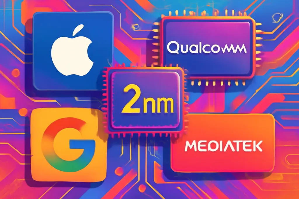
As TSMC’s 2nm production timeline solidified through early 2025, major fabless companies began making critical strategic decisions that would determine their competitive positioning for the 2026 device launch cycle. Each company’s approach reflected not only their market priorities but also their assessment of the rapidly evolving foundry landscape as 2025 progressed.

Apple secures 50% of TSMC initial 2nm production.
Apple acted first and most decisively during the first half of 2025. By August 2025, the company had secured nearly 50% of TSMC’s initial 2nm production capacity for its A20 chip powering the iPhone 18 launching in fall 2026. This early commitment, made while competitors were still evaluating options, reflected Apple’s willingness to pay premium prices—TSMC’s 2nm wafers cost $30,000 per unit. Apple’s August 2025 allocation agreement ensures first access to technology that will deliver 15% faster performance and 30% better power efficiency when the iPhone 18 reaches consumers in late 2026.
Qualcomm is busy in multi foundry model
As Apple’s dominance of TSMC capacity became apparent by mid-2025, Qualcomm shifted toward a multi-foundry strategy. Rising TSMC costs and limited remaining capacity throughout the summer of 2025 pushed Qualcomm to hedge its bets across different suppliers. By September 2025, the company had begun developing dual versions of its Snapdragon 8 Elite 2—a standard 3nm version for TSMC production and a cost-effective 2nm variant for potential Samsung manufacturing. However, as Samsung’s yield struggles intensified through late 2025, uncertainty emerged about whether the Samsung variant would proceed to production.
Google might be late in 2nm race
Observing these supply chain constraints develop through 2025, Google made an increasingly bold strategic pivot. During the second half of 2025, Google finalized plans to leapfrog from its current 4nm Tensor processors directly to 2nm with the Tensor G6 for Pixel 11 in 2026. This decision, representing a dramatic departure from Google’s historically conservative approach to process adoption, was finalized as 2025 drew to a close and could position Google ahead of Qualcomm’s now-uncertain 2nm timeline.
Samsung is going internal for its 2nm plans
Meanwhile, as external foundry options became more constrained through 2025, Samsung’s mobile division reinforced its commitment to vertical integration. Despite mounting evidence of yield challenges at Samsung Foundry throughout the year, the mobile division maintained its plans to use the Exynos 2600 on Samsung’s SF2 process for the Galaxy S26 series launching in early 2026. This strategy, while offering cost advantages, became increasingly high-stakes as Samsung Foundry’s 2nm struggles persisted into the final quarter of 2025.
As 2025 concluded, these divergent strategies set the stage for an unprecedented competitive battle in 2026. The strategic positions established during 2025—Apple’s guaranteed TSMC supply, Google’s aggressive leap to 2nm, Qualcomm’s multi-foundry hedge, and Samsung’s vertical integration bet—will determine competitive advantages when AI-powered devices utilizing 2nm’s superior efficiency reach consumers through 2026 and 2027.
The strategic chess moves made throughout 2025 illustrate how 2nm represents more than a process advancement—it became a pivotal moment that reshaped industry partnerships and competitive positioning for the AI-driven computing era ahead.
Discover more from WireUnwired Research
Subscribe to get the latest posts sent to your email.


