What comes to your mind when I say: name three inventions that changed the semiconductor industry in its totality?
Probably you would think of the transistor, the integrated circuit, or maybe EUV lithography, right?
But what if I tell you that’s not the whole story. Behind the scenes, there have been several lesser-known inventions that quietly reshaped the entire semiconductor landscape — enabling faster chips, longer battery life, and continued innovation even when Moore’s Law seemed to hit a wall.
In this detailed WireUnwired article, I’ll explore three such underrated inventions that, though often overlooked, changed the semiconductor industry forever.
3 Lesser known inventions that made semiconductor industry what it is today .
1. CMOS Technology (1963–1980s): The Enabler of Low-Power Chips.
Today whenever any SOC comes in the market , the designing company be it Snapdragon or Mediatek or Apple Silicon often talks about how much power efficient their this new generation chipset is when compared to previous ones. But have you really though when did this all started .
Well the real breakthrough happened long time ago — in 1963, when Frank Wanlass at Fairchild Semiconductor introduced CMOS technology.
CMOS stands for Complementary Metal-Oxide-Semiconductor, and it did something revolutionary: it drastically reduced the power consumption of integrated circuits. Unlike other logic families of the time, CMOS only consumed power when switching states — not while idle. That simple property made it the perfect choice for battery-operated devices and, eventually, for everything from watches and calculators to smartphones and servers.

By the 1980s, CMOS had quietly taken over the industry. While NMOS and bipolar logic faded out, CMOS became the backbone of low-power chip design — setting the stage for the mobile revolution, wearable tech, and even energy-efficient data centers.
Today, whether you’re scrolling Instagram or running an AI model on your phone, you’re using CMOS — without even realizing it.
TRENDING
2. Copper Interconnects & CMP (1990s): The Infrastructure That Made Chips Faster

We often credit faster chips to smaller transistors, but few realize that as transistors shrank in the 1990s, it wasn’t the logic that became the bottleneck — it was the wiring.
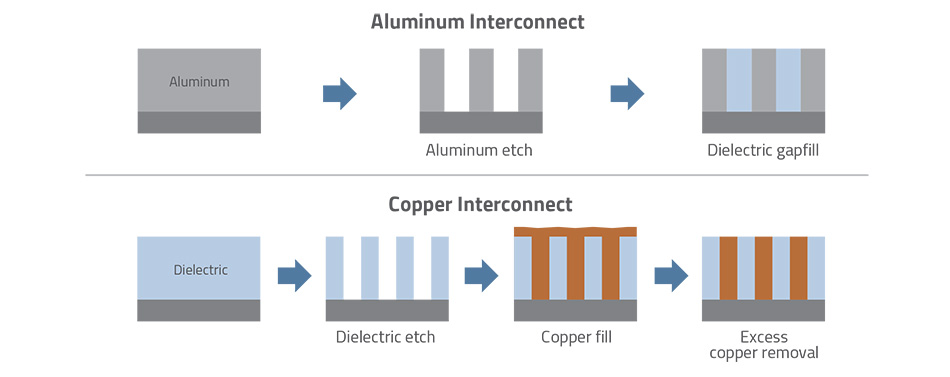
Back then, most chips still used aluminum interconnects, which simply couldn’t keep up. As chip complexity exploded, aluminum lines became too resistive and slow. That’s when IBM engineers introduced a two-part solution that quietly redefined chip performance:
🔹 Copper Interconnects
🔹 Chemical Mechanical Polishing (CMP)
Copper, with its lower resistance, allowed electrons to move faster, reducing delays. But copper alone wasn’t enough. To stack multiple layers of wiring reliably, chips needed ultra-flat surfaces — which is where CMP came in. This process polished the wafer to a near-perfect flatness between each layer, enabling the creation of today’s multi-layer, high-density chip architectures.
Together, these two under-the-hood innovations paved the way for GHz-class processors and helped extend Moore’s Law without shrinking transistors. Without copper and CMP, the chips powering everything from early Pentiums to modern AI accelerators would’ve hit a wall far earlier.
In essence, this was semiconductor civil engineering — and it changed everything.
3. FinFET Transistors (2000s–2010s): Moore’s Law Saviour

As the semiconductor industry pushed below 45nm in the mid-2000s, and then below 30nm in the early 2010s,traditional planar transistors began to show cracks — not physical, but electrical. Leakage currents soared, power consumption exploded, and the scaling curve that had driven decades of innovation started to flatten.
That’s when researchers at UC Berkeley, around the year 2000, proposed something bold: FinFETs — a new kind of transistor that stood vertically on the chip, like a fin rising from a flat surface.
Unlike planar designs, FinFETs allowed the gate to wrap around the channel on three sides, giving better control over current flow and drastically reducing leakage. It was elegant, clever, and incredibly effective.
Intel was the first to commercialize FinFETs at the 22nm node in 2011, calling it a “3D Tri-Gate transistor.” Soon after, the rest of the industry followed. FinFETs became standard across mobile SoCs, CPUs, and high-performance GPUs — quietly powering flagship smartphones, data centers, and AI chips alike.
Also Read :Deep dive into Intel’s new Backside power delivery
In a way, FinFETs weren’t just a new transistor — they were a design hack that gave Moore’s Law a second wind, just when the industry needed it most.
Conclusion
While the spotlight often shines on transistors and EUV scanners, the semiconductor industry owes just as much to the quiet, underrated innovations that kept the momentum going. From CMOS unlocking low-power devices, to copper wiring and CMP enabling GHz-class performance, to FinFETs rescuing Moore’s Law from collapse — each of these inventions changed the game in ways most people never see.
These aren’t just engineering tweaks. They’re the invisible breakthroughs that made your phone thinner, your servers faster, and your chips smarter. And in an industry racing toward angstroms and AI, remembering these foundational shifts isn’t just useful — it’s essential.
Discover more from WireUnwired Research
Subscribe to get the latest posts sent to your email.


