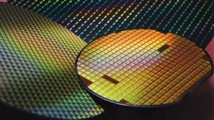
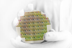
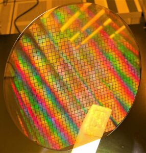
Wafers, those thin slices of magic, are the foundation of modern electronics. From smartphones to solar panels, these silicon marvels form the base for integrated circuits, the tiny brains of our devices. But did you know there’s a whole world beyond silicon wafers? Let’s delve into the fascinating realm of wafer types and explore their unique properties.
Silicon Wafer: The Unsung Heroes of semiconductor wafers
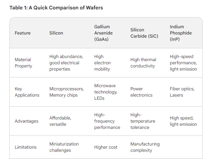
Silicon, the most abundant element on Earth after oxygen, takes center stage in wafer form. Grown using the Czochralski process, where a molten silicon seed slowly pulls a crystal upwards, these wafers boast a perfect crystalline structure. This makes them ideal for transistors, the building blocks of integrated circuits. Their affordability and versatility have cemented their position as the backbone of the electronics industry.
However, silicon wafers have limitations. As miniaturization reaches its physical limits, packing more and more transistors onto a chip becomes increasingly challenging. This is where other wafer types come into play.
Dr. Lisa Su, CEO of AMD, aptly states, “The future of computing relies on constant innovation in materials science.” New wafer materials are being explored to push the boundaries of performance and efficien

Gallium Arsenide (GaAs) Wafer: Speed Demons of semiconductor wafers
Gallium arsenide (GaAs) wafer offer several advantages over silicon. They boast superior electron mobility, allowing for faster signal transmission. This makes them ideal for high-frequency applications like microwave circuits and radiofrequency (RF) devices used in mobile communication. Additionally, GaAs wafers excel in applications requiring high-power handling, such as solar cells for space satellites.
However, GaAs wafer come at a cost. They are significantly more expensive to produce compared to silicon, limiting their widespread adoption in consumer electronics.

Silicon Carbide (SiC) Wafers: Power Players
Silicon carbide (SiC) wafer is gaining traction due to their exceptional properties. They can withstand higher temperatures and voltages compared to silicon, making them ideal for power electronics. This translates to significant efficiency gains in applications like electric vehicles and renewable energy systems.
SiC wafer also offer superior radiation resistance, making them suitable for harsh environments like aerospace and nuclear power plants.
The main hurdle for SiC wafer is their complex manufacturing process, leading to higher costs. However, as research and development efforts intensify, SiC wafers are expected to become more cost-effective, paving the way for wider adoption.


A Glimpse into the Future: Beyond Silicon
While silicon, GaAs, and SiC are the most prominent wafer types, researchers are exploring other materials with unique properties. Here’s a brief look at some emerging contenders:
- Indium phosphide (InP): Offers exceptional light-emitting properties, making it a potential candidate for high-performance lasers and optical devices.
- Gallium nitride (GaN): Showcases excellent efficiency in converting electricity to light, making it a promising material for next-generation LEDs.
These are just a few examples, and the future of wafer technology is constantly evolving.
Conclusion
The world of wafer extends far beyond the ubiquitous silicon. Each wafer type possesses unique strengths and weaknesses, making them suitable for specific applications. As technology demands continue to evolve, research into novel wafer materials promises to unlock even greater possibilities. From faster processors to more efficient power grids, these thin slices of innovation are shaping the future of technology.
Discover more from WireUnwired Research
Subscribe to get the latest posts sent to your email.


