⚡ WireUnwired Research • Key Insights
- The News: Apple has reportedly secured 100% of the initial capacity for TSMC’s upcoming 2nm (N2) node. Yes, all of it.
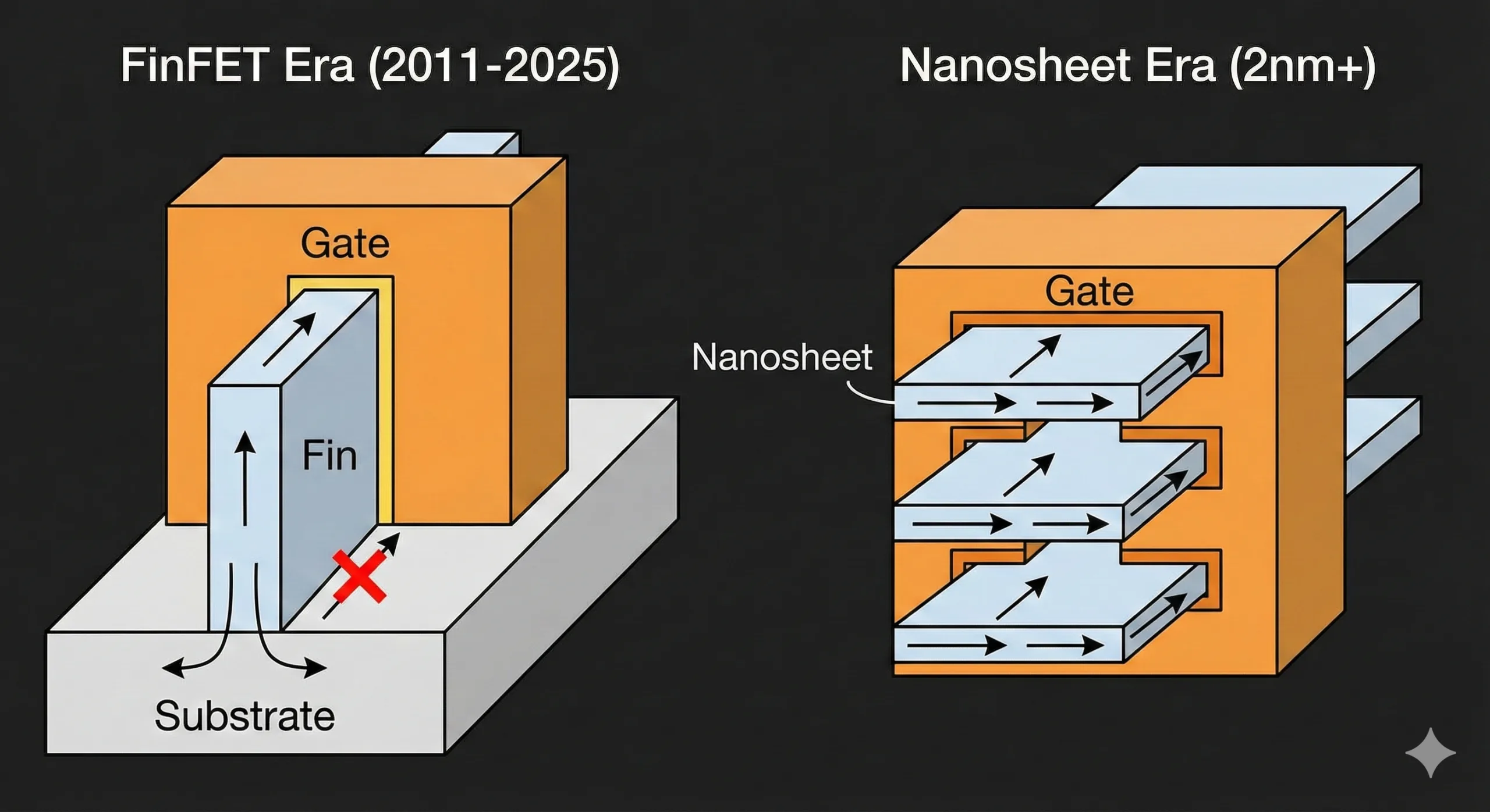
- The Shift: This marks the end of the 15-year FinFET era. The physical shape of the transistor is changing from a vertical “Fin” to horizontal “Nanosheets” (Gate-All-Around).
- The Why: At 3nm, FinFET transistors became too “leaky.” The new shape allows for 4-sided control, solving the power leakage problem.
The “All-In” Bet on 2nm
When TSMC announces a new process node, it usually triggers a bidding war. NVIDIA, AMD, Qualcomm, and Apple all fight for their slice of the pie. But this year, the war is already over.
Reports indicate that Apple has effectively cleared the table, buying TSMC’s entire initial run of 2nm chips.
Why such an aggressive move? Because the iPhone 17 Pro won’t just need to run apps; it will need to run On-Device AI models. To do that without melting the battery, Apple needed a fundamental shift in physics.
The Physics Problem: The Leaky Hose
If you look at the processor inside your current phone (iPhone 16 or Galaxy S25) under a microscope, you will see a forest of “Fins.”
For 15 years, the FinFET (Fin Field-Effect Transistor) has been the king of silicon. It looked like a shark fin sticking up from the chip, allowing electricity to flow through it.
Why change the shape? Because of Leakage.
Imagine a garden hose (the channel) that you are trying to pinch shut (the Gate) to stop water (electrons) from flowing.
- Planar Transistors (Old School): You pinched the hose from the Top (1 side).
- FinFET (Current Era): You pinched the hose from the Top, Left, and Right (3 sides).
This was great… until we got to 3nm. At that size, the “Fin” became so narrow and wobbly that the Gate couldn’t pinch it tight enough anymore. Electrons started leaking through the bottom, even when the chip was off. This is why your phone battery drains in your pocket.
The Solution: Gate-All-Around (GAA)
But as of today, the King is dead. The “Nano-Sheet” has arrived.
The new 2nm chips use Gate-All-Around architecture (TSMC calls it Nanosheet). Instead of a Fin sticking up, the transistor is now a stack of horizontal sheets “floating” in air. The Gate wraps around them completely—Top, Bottom, Left, and Right.

The efficiency of a transistor is defined by its Subthreshold Swing (\(SS\))—basically, how hard is it to turn the switch fully “Off”? The ideal physical limit at room temperature is 60 mV/decade.
With FinFET (3-sided control), as we shrunk the gate length (\(L_g\)), the control weakened due to Short Channel Effects:
$$SS_{FinFET} \approx 60 \times (1 + \frac{C_{depletion}}{C_{oxide}})$$
Because the Gate couldn’t touch the bottom of the Fin, the control capacitance ($C_{oxide}$) wasn’t high enough. The switch was leaky.
With GAA (4-sided control):
$$C_{oxide} \rightarrow \text{Maximized}$$
By wrapping the fourth side, we maximize electrostatic control. This brings the SS value back down near the ideal limit of 60, meaning the chip stops leaking current. B-)
The WireUnwired Takeaway
Apple didn’t just buy a “smaller” chip. They bought a “tighter” switch.
The shift to 2nm isn’t about fitting more transistors; it’s about regaining control over them. The Fin is dead. Long live the Sheet.
Discover more from WireUnwired Research
Subscribe to get the latest posts sent to your email.


