Assessing materials at deeper levels with enhanced resolution is essential in areas like high-energy physics, quantum materials, nuclear energy production, biomedical diagnostics, and aviation. Conventional techniques, such as radiographic (X-ray) testing, offer high resolution but struggle with penetration in solid materials and utilize ionizing radiation, which can be expensive and less feasible for broad application.
A significant breakthrough has been achieved by the Indian Institute of Technology (IIT) Madras in India and Intelligent Optical Systems in the USA regarding material evaluation by combining high-resolution ultrasonic imaging with advanced micro-metalenses, the team has successfully addressed the shortcomings of traditional imaging methods, facilitating easier detection of internal defects within solid materials.
Limitations of Conventional Imaging Technologies
Conentional methods used for material evaluation included the use of X Rays and Ultrasound. Although X Rays can penetrate deeper into materials, prolonged radiation exposure can be harmful to human health. Ultrasonic imaging can be non-ionizing, cost-effective, and can penetrate deeper inside the materials. But its longer wavelength does not allow to detect microscopic defects.
This innovative research bridges that gap by introducing silicon-based micro-metalenses, it enhances ultrasonic resolution and enabling the visualization of deeper and finer structures.
Breaking the Diffraction Barrier using metalenses
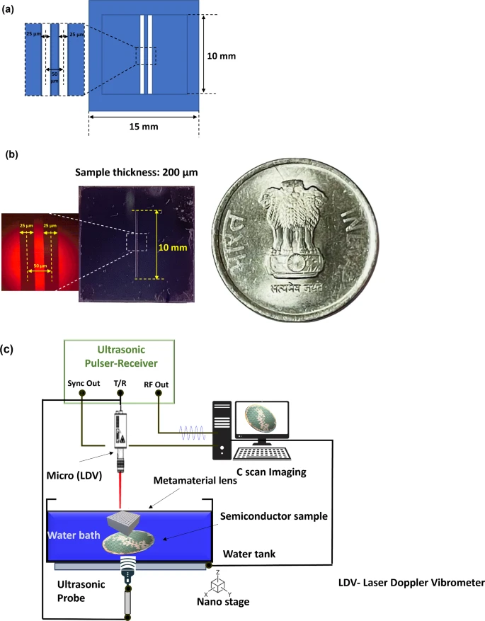
This research overcame a fundamental constraint on imaging resolution which is “diffraction limit ” . The research team created advanced silicon-based metalenses with carefully designed 10-micron square holes. These metalenses, combined with a micro-focal laser that can detect tiny sub-micron spots, it has greatly improved defect visibility. During experiment resolution of 50 microns was achieved , it will help in detecting slit like defects .
Precision Engineering: The Imaging Setup
The study’s success depended on a carefully designed setup. An ultrasonic transmitter on a computer-controlled scanning stage worked with a laser receiver to turn movement data into high-resolution ultrasonic signals.
Silicon samples embedded with the micro-metalenses were immersed in water tanks for imaging. Advanced fabrication techniques, such as deep reactive ion etching (DRIE), were employed to create the micron-scale holes. To enhance signal reflectivity, the metalenses were coated with gold. Additionally, oxidizing the channels within the metalenses ensured hydrophilic properties, maintaining stable water levels and enabling consistent detection.
Impressive Imaging Capabilities
The system clearly detected the defects, which were 50 microns apart. Some minor side effects appeared in the B-scan profile, but the signal quality was excellent, which allowed accurate identification of defects. Finite element (FE) simulations also confirmed the improved resolution, which mainly depends on the design of the metalenses.

Far-Reaching Industrial Applications
This research can help in increasing the potential of many industries. Applications include non-destructive evaluation (NDE) in manufacturing, biomedical imaging, and diagnostics for electronic materials. Important sectors such as aviation, nuclear power, and quantum material research will also get benefits from this research work. It will help in getting safer, more precise, and cost-effective diagnostic solutions.
The Future of Ultrasonic Imaging
This research marks the beginning of a new chapter in high-resolution imaging. Future advancements in this method will broaden the scope of this technology.
Discover more from WireUnwired Research
Subscribe to get the latest posts sent to your email.


