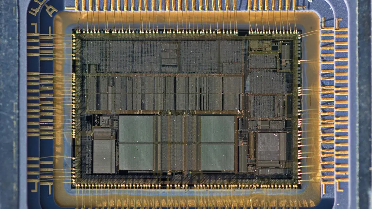
Semiconductor fabrication has always been a fascinating task for engineers. It’s just so exciting to imagine how billions of transistors are fitted into a chip even smaller than a human fingernail. In this very article we are gonna understand completely how a semiconductor is fabricated. But before we start let us have a brief about semiconductors.
We as humans have much flexibility in terms of language that we can use ,we have English ,Hindi ,French ,Spanish and so on ….. But when it comes to the digital world , we have a single language and that language too have just Two words or more precisely Bits: 1 and 0. The whole digital world is just a play of just these two bits .The 0s and 1s constantly shape the way we interact with technology and with each other on a daily basis – and the beating heart of this binary revolution is the semiconductor device.
What are Semiconductors ?
As defined earlier these semiconductors are the beating heart of Binary Revolution. Just like a Water gauge can be used to control the flow of water,a semiconductor device can be used to control the flow of electricity with Great precision. So , we can define semiconductors as devices that sometimes can act as conductors and sometimes as insulators depending upon the situations.
Also read: IISc Bengaluru Team designs alternative to semiconductors that have much more efficiency.
When we talk about Semiconductors , we talk about its most important and fundamental type i.e Transistors. Let me tell you when the first Integrated Circuit (I.C) was made it only had Four(4) transistors and it was sufficient to do basic arithmetic tasks and now we put somewhat Billions of Transistors in a single chip .By just these numbers you can imagine how far we have come and how far we have to go.
As I discussed at the very starting of this article , the world of fitting these Billions of Transistors into a single chip which is even less than the size of a human fingernail is so much fascinating , but at the same time it requires too much of precision. For instance, the accuracy required is equivalent to dividing a strand of human hair into a thousand segments each of specific width, and further subdividing each segment into a hundred parts. This is why fabricating semiconductors involves cutting-edge technology and science.
Now we are so close towards our topic of Discussion.
How Is Semiconductor Fabrication Done?
The process of Semiconductor Fabrication starts with an engineer carefully selecting a silicon wafer as the foundation on which the whole semiconductor will be built. Then a team puts silicon(the building block of Semiconductors), sourced from sand, through extremely carefulness to separate it from other substances which are mostly impurities that come with Silicon, until they have an ultra-pure wafer with impurity levels as low as a few parts per billion. (This percentage is comparable to an error of merely 1 cm when measuring the earth’s diameter.)
Also Read : Semiconductor Developers May Earn 3 Times Salary as of a Software Developer
Next Step is the photolithography process – This is the step after which we have a carved layout on our Silicon Wafer. The wafer is then coated with a light-sensitive material called a Photoresist. Then, a mask is held in front of the wafer and light is shined on it. The mask contains small gaps in the shape of the circuit pattern. The light passes through these gaps and erodes the underlying parts of the photoresist. As a result, the photoresist on the wafer ‘acquires’ the pattern of the transistor circuits.
Following photolithography, engineers use chemical and/or physical techniques to remove the uncarved parts of the photoresist, leaving behind the circuit’s structure on the silicon substrate.
Then they dope the semiconductor – i.e. Knowingly add impurities to specific parts of the semiconductor to alter its electrical properties(i.e to make these semiconductors P Type or N Type), and deposit thin layers of materials such as metals or insulators to the wafer’s surface to form electrical connections or insulate components. Then the resulting product is packaged – individual chips are separated, encapsulated, and tested to make sure they’re functional and reliable – and finally integrated into electronic devices.
Join Our WhatsApp Community to connect with Like Minded Individuals.
Machines Used For Semiconductor Fabrication.
Conclusion.
Discover more from WireUnwired Research
Subscribe to get the latest posts sent to your email.


I am always searching online for posts that can assist me. Thx!