Key Insights
- onsemi launches vertical GaN semiconductors built on proprietary GaN-on-GaN technology, enabling higher voltages, faster switching, and greater power density for AI data centers and electric vehicles.
- Devices offer nearly 50% lower energy losses and are about three times smaller than lateral GaN, with initial 700V and 1,200V units sampled to early customers.
- Manufacturing is centered in Syracuse, NY, backed by over 130 patents, strengthening local innovation and competitiveness.
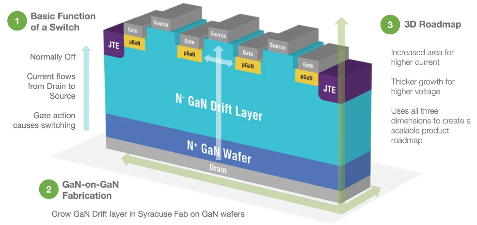
Onsemi has launched its vertical GaN semiconductors ,announced on October 30, 2025 it marks a significant leap for power electronics, targeting critical sectors such as AI infrastructure, electric vehicles, renewables, and aerospace specially in India. Built on proprietary GaN-on-GaN technology, these next-generation devices conduct current vertically, allowing for higher operating voltages, faster switching speeds, and greater power density compared to traditional lateral GaN chips. According to Stock Titan’s coverage, onsemi claims its vGaN devices can reduce energy losses by nearly 50% and are approximately three times smaller than current lateral GaN alternatives.
About onsemi
onsemi (formerly ON Semiconductor) is a global leader in intelligent power and sensing technologies, delivering advanced semiconductor solutions for energy-efficient electronics. The company’s portfolio spans power management, automotive, industrial, and cloud markets, with a strong focus on high-performance silicon, silicon carbide (SiC), and now vertical GaN devices. onsemi partners with leading innovators in electric vehicles, renewable energy, AI data centers, and industrial automation to drive next-generation electrification and intelligent infrastructure worldwide.
Why OnSemi’s Vertical GaN Matters ?

Gallium Nitride (GaN) is a wide-bandgap semiconductor that has rapidly reshaped modern power electronics. Compared to traditional silicon, GaN switches faster, operates at higher voltages, and delivers greater efficiency—all while reducing size and weight. These advantages have already made GaN essential in fast chargers, renewable inverters, and efficient power supplies.
Now, onsemi is taking this performance leap even further with vertical GaN. The move to vertical GaN architecture is driven by surging energy demands from AI data centers and the electrification of transport. By conducting current vertically through the semiconductor, these chips can handle much higher voltages—onsemi is already sampling 700V and 1,200V units to select customers. This design enables more compact and efficient systems, which is crucial for space-constrained applications like electric vehicles and dense AI server racks. As highlighted by onsemi’s official press announcement, the new technology sets a benchmark for efficiency, power density, and ruggedness, supporting the next wave of electrification and intelligent infrastructure.
How Does onsemi’s Vertical GaN Compares to lateral GaN ?
| Feature | Vertical GaN (onsemi) | Lateral GaN |
|---|---|---|
| Current Direction | Vertical (through substrate) | Lateral (across surface) |
| Operating Voltage | Up to 1,200V (sampled) | Typically <700V |
| Efficiency | ~50% lower losses | Standard losses |
| Size | ~3x smaller | Larger footprint |
| Key Applications | AI data centers, EVs, renewables, aerospace | Industrial, consumer |
Local Innovation and Global Impact of Onsemi’s Vertical GaN Launch.
Manufacturing and R&D for these devices are based at onsemi’s Syracuse, NY facility, amplifying the region’s status as a hub for advanced semiconductor innovation. The company’s vertical GaN technology is protected by a portfolio of over 130 patents, covering everything from process advancements to device architecture and systems integration. Regional and national outlets have emphasized the role of the Syracuse fab in driving local economic growth and strengthening U.S. competitiveness in high-tech manufacturing, as noted in Barchart’s report.
Industry Reaction and Market Context
Industry observers are optimistic about the disruptive potential of onsemi’s vGaN semiconductors. The combination of substantial efficiency gains and miniaturization could reshape power electronics for AI infrastructure, EVs, and renewables. The global power GaN device market is forecasted to grow at a 42% CAGR, reaching $3 billion by 2030, according to Compound Semiconductor, positioning onsemi’s technology at the forefront of a rapidly expanding field.
Join the Conversation
Stay ahead of semiconductor breakthroughs: Join WireUnwired Research on WhatsApp or connect with peers on WireUnwired Research on LinkedIn for tech news and analysis.
“Built on novel GaN-on-GaN technology, onsemi’s vertical GaN architecture sets a new benchmark for power density, efficiency and ruggedness.” — onsemi press announcement
Discover more from WireUnwired Research
Subscribe to get the latest posts sent to your email.


